mandelFPGA
introduction
Field-programmable gate arrays (FPGAs) are interesting devices. They are (re)programmable logic on a chip - pretty much any digital circuit can be implemented on a FPGA of sufficient size. They are widely used for prototyping, custom one-off circuits, and short production runs unlikely to benefit from the lower unit cost of an application-specific integrated circuit (ASIC).
Most fascinating, potentially, is their use for computation. A dirty little secret about general-purpose CPUs is that they are actually rather slow for specific computing tasks. Graphics cards, for instance, can perform numerical computations at a far greater rate than a processor of the same era, as they are designed for the specific purpose of high computational throughput. CPUs, on the other hand, are better at more generic tasks but do comparatively poorly in floating-point throughput. FPGAs, with their virtually unlimited reconfigurability, are a useful addition to a system containing task-specific chips and a general-purpose processor.
concept
Some time in the early 2000s, Joshua Wise had the idea to program a FPGA to draw a Mandelbrot set in real time. The Mandelbrot set is a connected set of points in the complex plane that depends on an infinite iterative process to determine whether each point is in the set. At each iteration, the original starting point is added to the (complex) square of the previous point. If the result of the iteration never 'escapes' to infinity, the original point is part of the Mandelbrot set. The number of iterations determines the detail in the resulting render; typically, a hundred iterations are sufficient to render a view of the entire set such that the artifacts are smaller than a pixel.
Years later, we had learned a thing or two about digital logic and began to prototype the circuit. We quickly realized that it would be a very computationally intensive task. At 640x480 resolution and 60 frames per second, we need to output fully-computed pixels at 25MHz (including the overhead of vblank and hblank for the VGA signal). Each iteration requires three multiplications to compute the square of the current value and several comparisons to determine if it's part of the set; 25 million pixels that each require dozens of iterations must be computed every second.
pipelines: not just for oil and gas
The key to high throughput is to pipeline the computation. If we create a circuit that can compute one iteration per clock cycle, we can duplicate it ten times to compute ten iterations per cycle. Rather than placing the units in parallel, we put them in series like an assembly line or bucket brigade, forming a type of computational pipeline called a linear systolic array. Each unit computes one iteration and passes it along to the next one. This way, while each pixel spends many clock cycles in the pipeline, the overall throughput is one pixel per clock. The entire pipeline as implemented on our FPGA can easily be clocked at 25MHz, and thus real-time output is no problem.
While optimizing this pipeline, we realized that computing one entire iteration per clock cycle in each unit made inefficient use of the FPGA's logic resources. FPGAs are implemented as a reconfigurable fabric containing lookup tables tied to flip-flops; the number of flops and the amount of combinatorial logic that can feed them are in fixed proportion. To make each unit contain only one flop stage (single cycle) would make far more use of the lookup tables than the flops they are tied to. In the final design, then, each unit is itself pipelined to contain two stages: the first one contains three multipliers to compute a complex square, and the second performs the comparisons to determine if the iteration has escaped. This let us clock the design almost twice as fast while using nearly the same overall resources.
more fasta
Although the pipeline could now run much faster, we needed a way to make use of the extra speed. At 50MHz, twice the required output speed, each pixel can actually be fed through the pipeline twice. This effectively doubles its length, computing double the iterations using the same logic. Using the 25MHz pixel clock as a control signal, the pipeline takes in a new pixel to be computed on the rising edge and a pixel from the end of the pipeline on the falling edge.
Eventually, we managed to further increase the frequency to 75MHz, which enabled triple-pumping the pipeline. Directly using the pixel clock to control the input to the pipeline would no longer work; we used a simple state machine to feed new, first pass, and second pass pixels into the pipeline in sequence.
miscellany
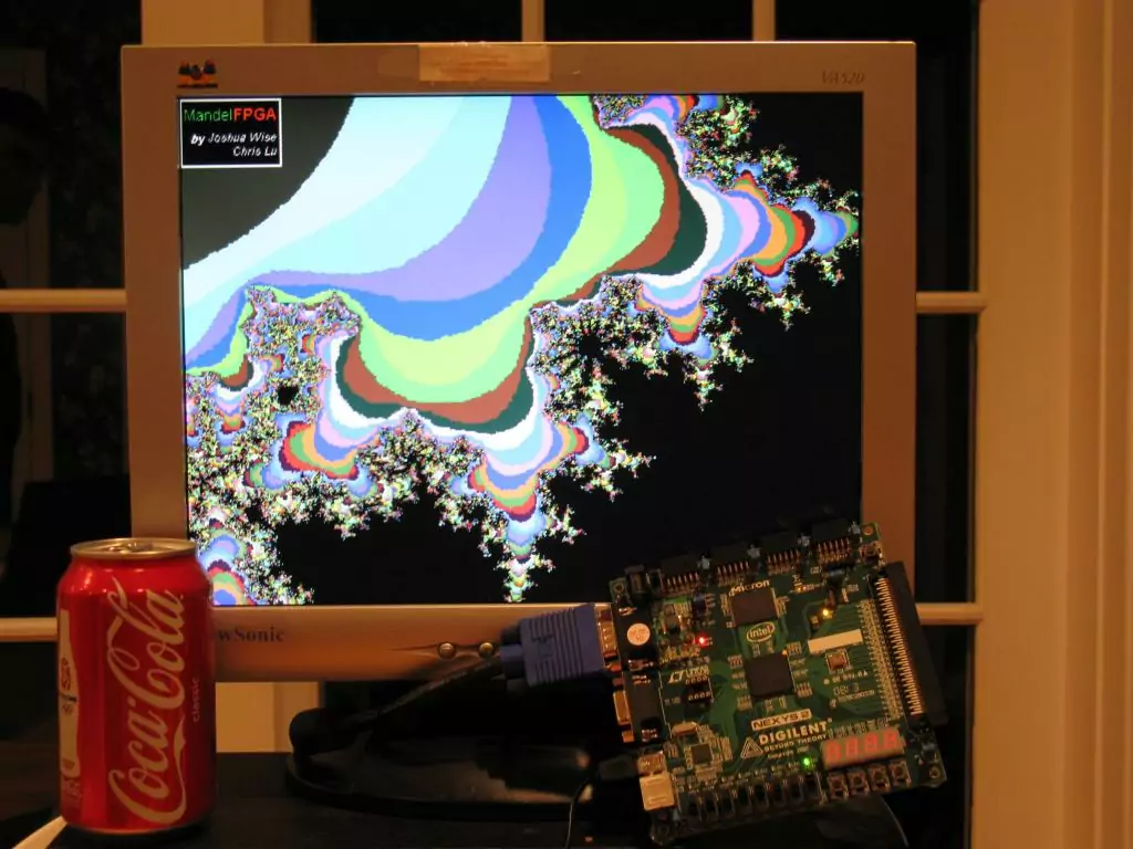
Some supporting modules were written to convert pixel locations into coordinates to feed into the pipeline and generate VGA output. We used the switches and buttons on the board to provide zoom (power of 2) and scroll capabilities. The output was colorized by directly swizzling the bailout iteration counter into RGB values, yielding the palette shown below.
final design
Using all but a few percent of the FPGA's logic resources, we could fit 22 triple-pumped iteration units for a 66-iteration pipeline, using 1.12 fixed-point arithmetic. This is a substantial level of computational power; if we regard each iteration as one 'operation' we already have 75MHz * 22 = 1.65 billion operations per second. Given that each iteration involves three multiplications and several additions and subtractions, the overall performance may be many billions of integer operations per second, comparable to modern CPUs.
Moreover, the FPGA used for the implementation is a low-end part. High-end chips (that cost more than a new car) are capable of much higher speeds and contain many times the logic resources. Were this code rewritten to take advantage of it, performance would easily outstrip by orders of magnitude the fastest processors, by any reasonable measure.
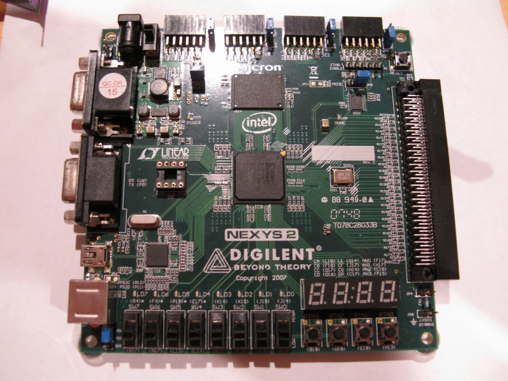 |
This is the board we are using, a Digilent Nexys-2 with a Xilinx XC3S1200E 1200k gate FPGA. '1200k gate' is some ASIC equivalent measure; the actual logic resources include about 9000 'slices' consisting of a four-bit lookup table and a flip-flop, plus dedicated multipliers, block RAM, I/O buffers, clocking modules, etc. |
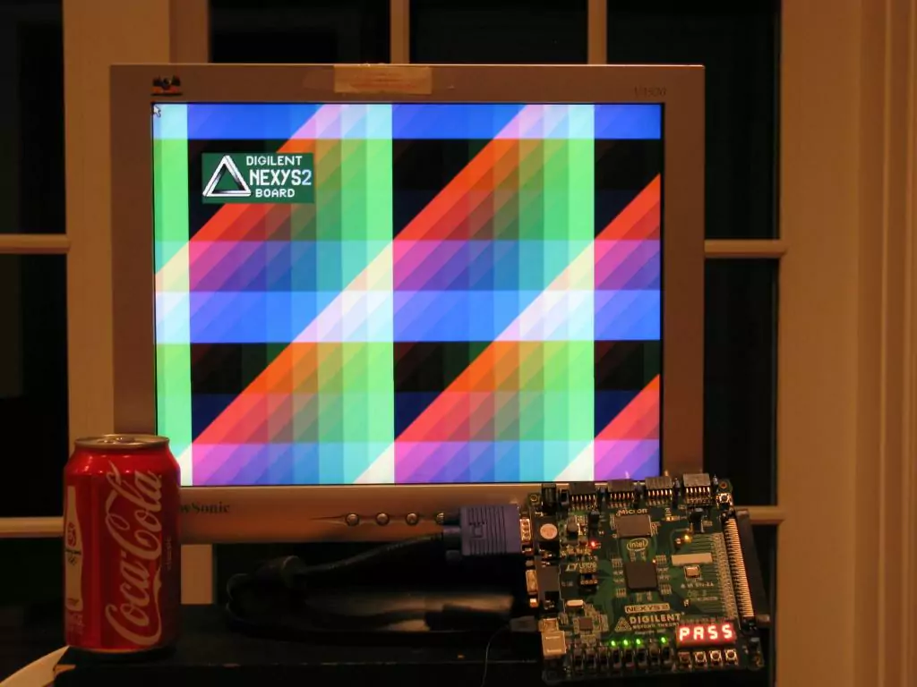 |
This is the default firmware. It does a number of interesting things with the board; the LEDs are controlled by the switches, the logo is draggable with a PS/2 mouse, and the buttons frob the 7-segment display. |
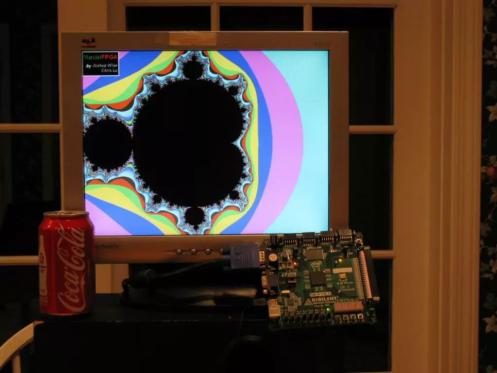 |
MandelFPGA running at the default zoom level. The center of the screen is 0 + 0i. It looks fairly clean despite the lack of anti-aliasing. |
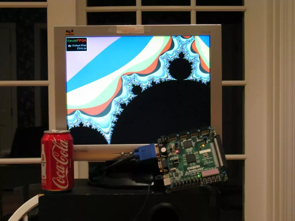 |
A photo showing the zoom and scroll capabilities. |
 |
This is the second highest zoom level. The edges start to become ragged and the smaller blobs lose definition due to the 66-iteration pipeline. |