LED wave array prototypes
The LED wave array went through a few iterations before the final design. I used LTSpice and the excellent Falstad circuit simulator to simulate the designs, but nothing can substitute for a real prototype. (Also, simulators are extremely slow at simulating large arrays.)
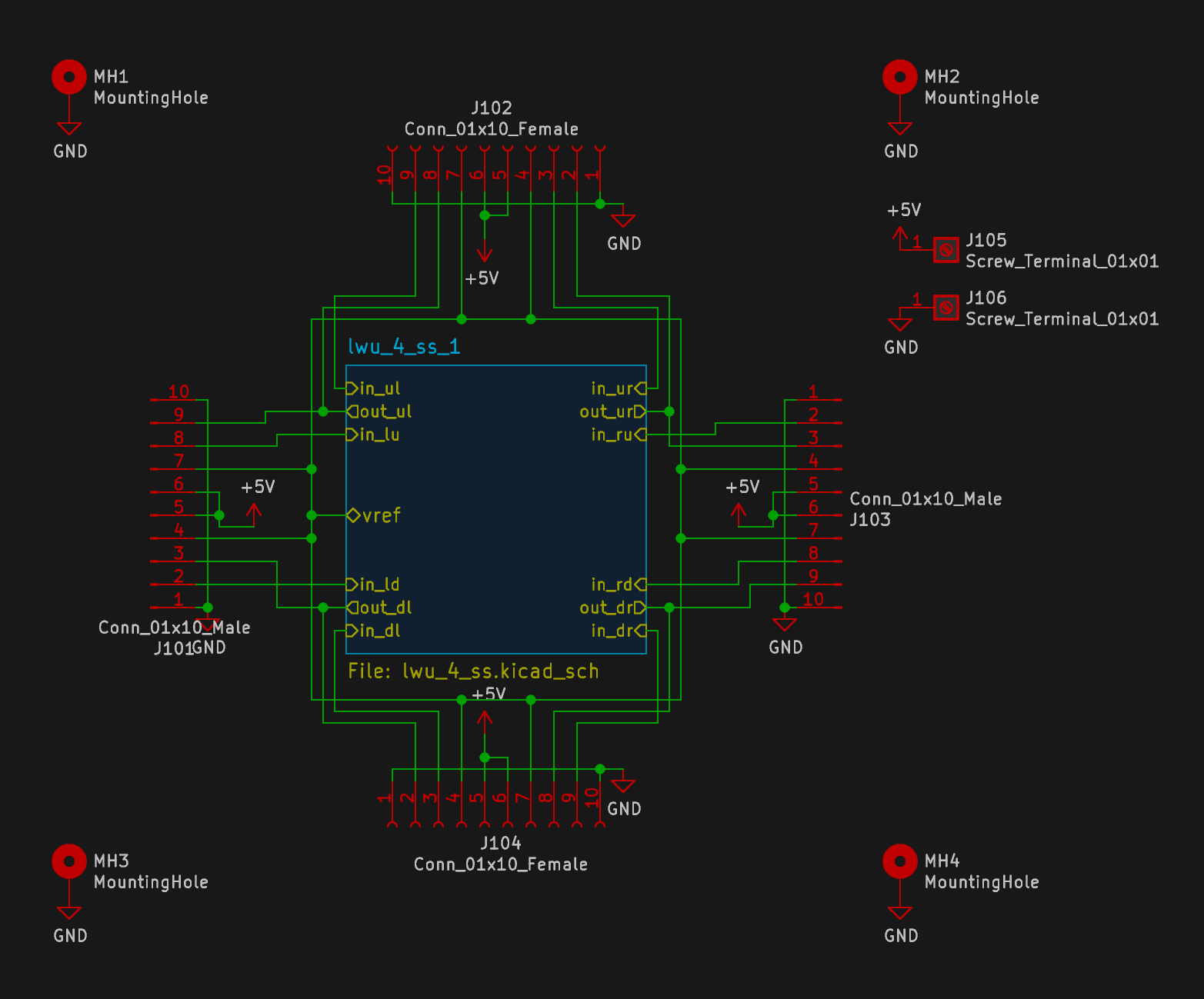
All of the prototypes use the same basic principle of a sensor driving a summing/double integrating opamp arrangement; for details, see the other page.
One unexpected advantage of waiting so long to start working on this project in earnest is that messing up has never been cheaper. Part of the reason I didn't get much further than the concept stage initially was that boards and components were expensive and difficult to get. But now, the hobby electronics scene has absolutely exploded, and the market with it. It used to be that to get PCBs, you either had to shell out on the order of $100 or break out the ferric chloride. Now it's ~$5 for ten production quality boards with silkscreen and soldermask from any number of Chinese PCB manufacturers. It would have been a dream come true for a 15-year-old me.
mark 1: linear array
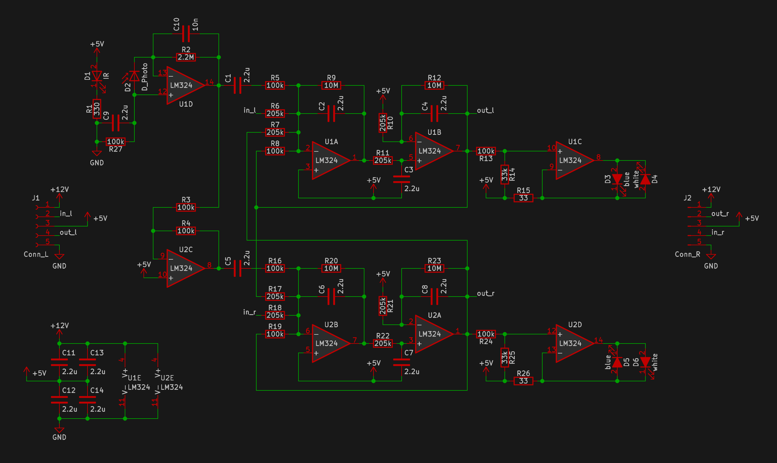 schematic
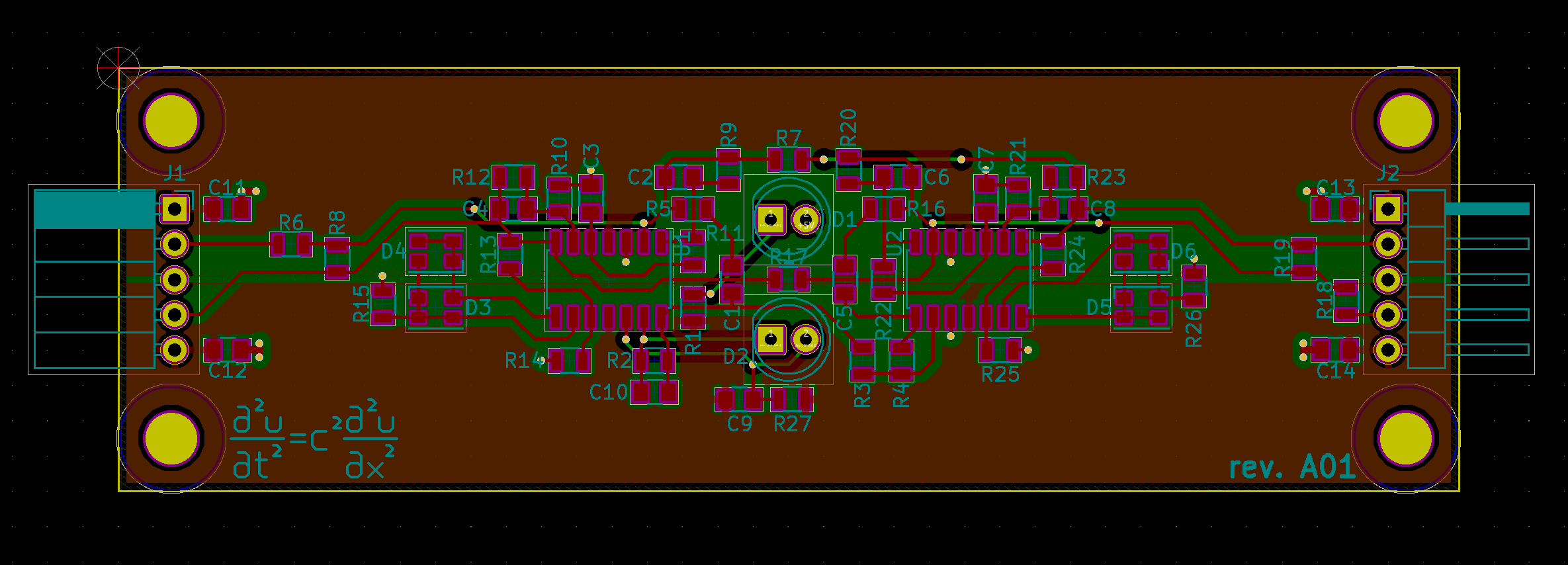 layout
 assembled board
The first prototype was a linear array with only two neighbors for each unit. It uses LM324 quad opamps instead of the low-voltage rail-to-rail LMV324 variant in later versions.
This prototype is very different from later versions and served to test an idea I was unsure about. This circuit uses one opamp in each unit as a current-regulated driver for pairs of LEDs in antiparallel. True current regulation allows the use of any color LED without having to worry about fine-tuning the supply voltage, allowing different color combinations in the same array as shown in the video. The disadvantage is that there is one fewer opamp available, forcing a cascade of design changes that ended up not working out so well.
To free up an opamp for the driver, we can use a noninverting integrator as the second integrator. The output will then be inverted and can be directly fed back into the summing integrator. However, this means that the output is inverted, forcing adjacent units to be entirely inverted for the summing behavior to be correct. As a single sensor feeds two units, its signal must be inverted when supplied to the other unit. This consumes the opamp that would otherwise generate the reference voltage. The circuit therefore needs a split supply.
I used a 12V rail split by a buck converter. It is important that this converter use synchronous rectification so it can sink current - the typical diode on the output will not allow current to flow back into it. The ability to sink current from the "middle" rail is the primary difference between a true split supply and an ordinary dual output supply. The converter is adjusted to around 5.5V as the LM324 opamps used have an asymmetric range; they are capable of approaching 0V closer than they can Vcc.
The LEDs do not fully turn off when idle; I suspect that the asymmetric split supply or part tolerances had something to do with it. I did not bother determining exactly why, because the design was unsatisfactory for other reasons - split supplies are uncommon, and the noninverting integrators took too many parts and were sensitive to tolerances.
The freedom to use any color is a significant advantage, and I believe this design can be made to work. I recently found that it is possible to make a summing double integrator with a single opamp, which would free up another opamp to use as a reference or even as a driver.
mark 2: 2D array
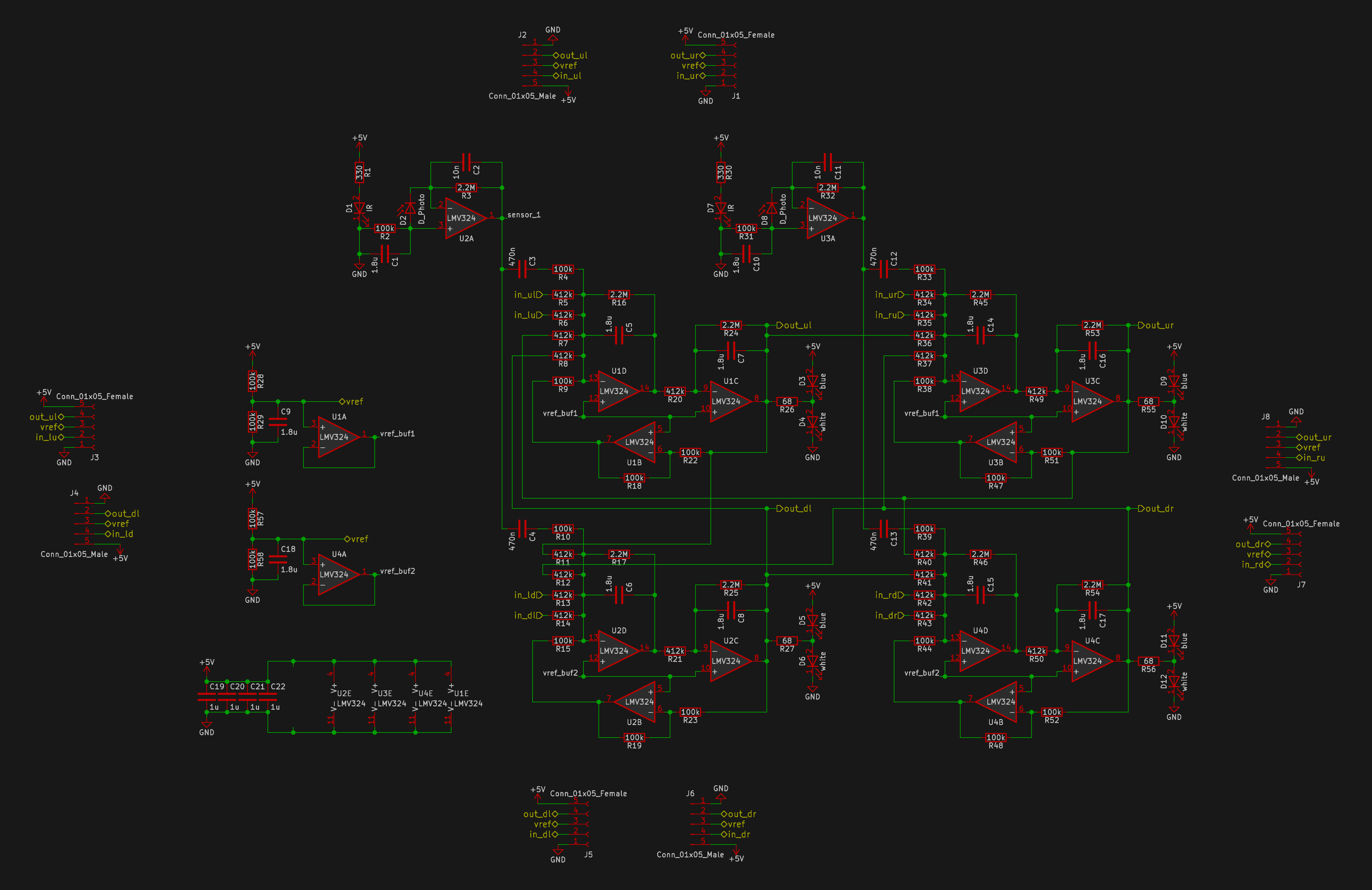 schematic
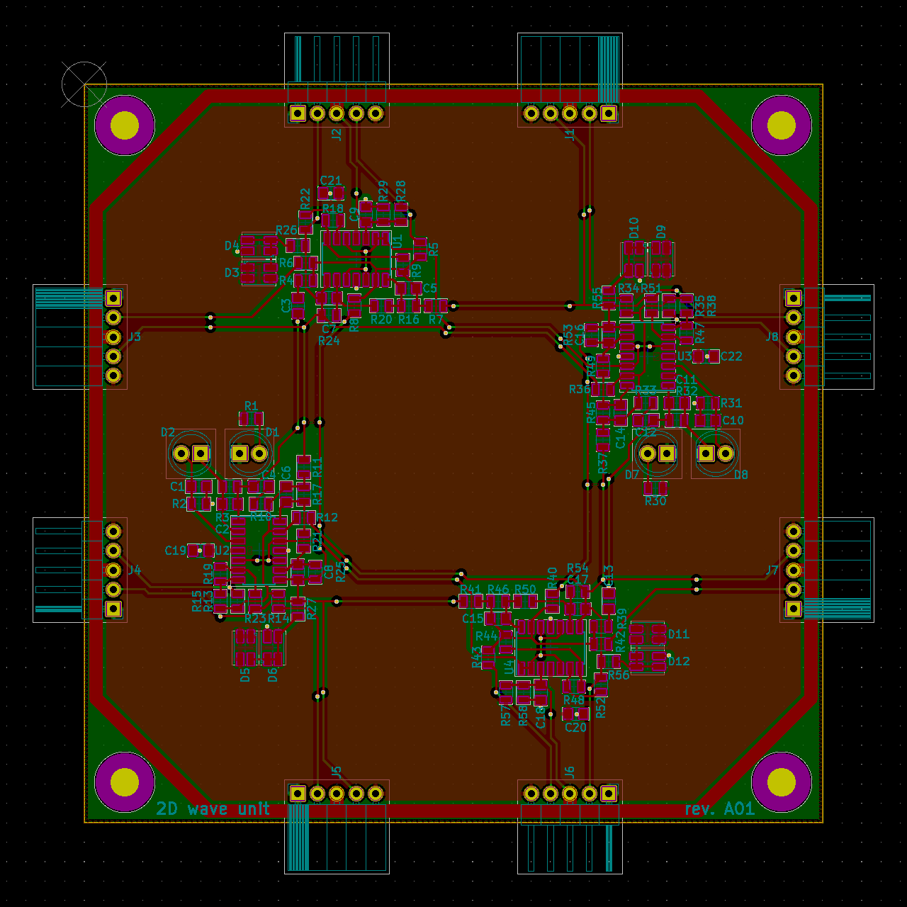 layout
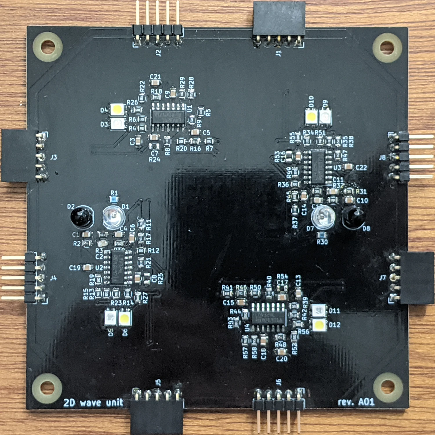 assembled board
The next one was a 2D array with four units per board. This design is much closer to the final one, with LMV324 opamps and a single 4.5V supply. The main differences from the final design are:
- some extra components, like a damping resistor on the second integrator and an extra resistor and capacitor in the photodiode amplifier
- lower gain on the photodiode amplifier (2.2Mohm)
- greater damping on the integrators (also 2.2M)
- reference voltage exported to other boards via edge connectors
The edge connectors are hermaphroditic so any edge can attach to any other edge. Rotating every other board 90 degrees spreads the sensors out and gives more uniform coverage; this pattern is also used in the final design.
I hand soldered all 100 components per board for all 10 boards. I got very fast at soldering 0805s with two soldering irons, but I never want to do that again.
This version was an extremely useful testbed for playing with component values to get the desired behavior. I also tried removing the suspected extraneous components which let me reduce the parts count significantly in the next version.
mark 3: 2D array, optimized
 schematic (top level)
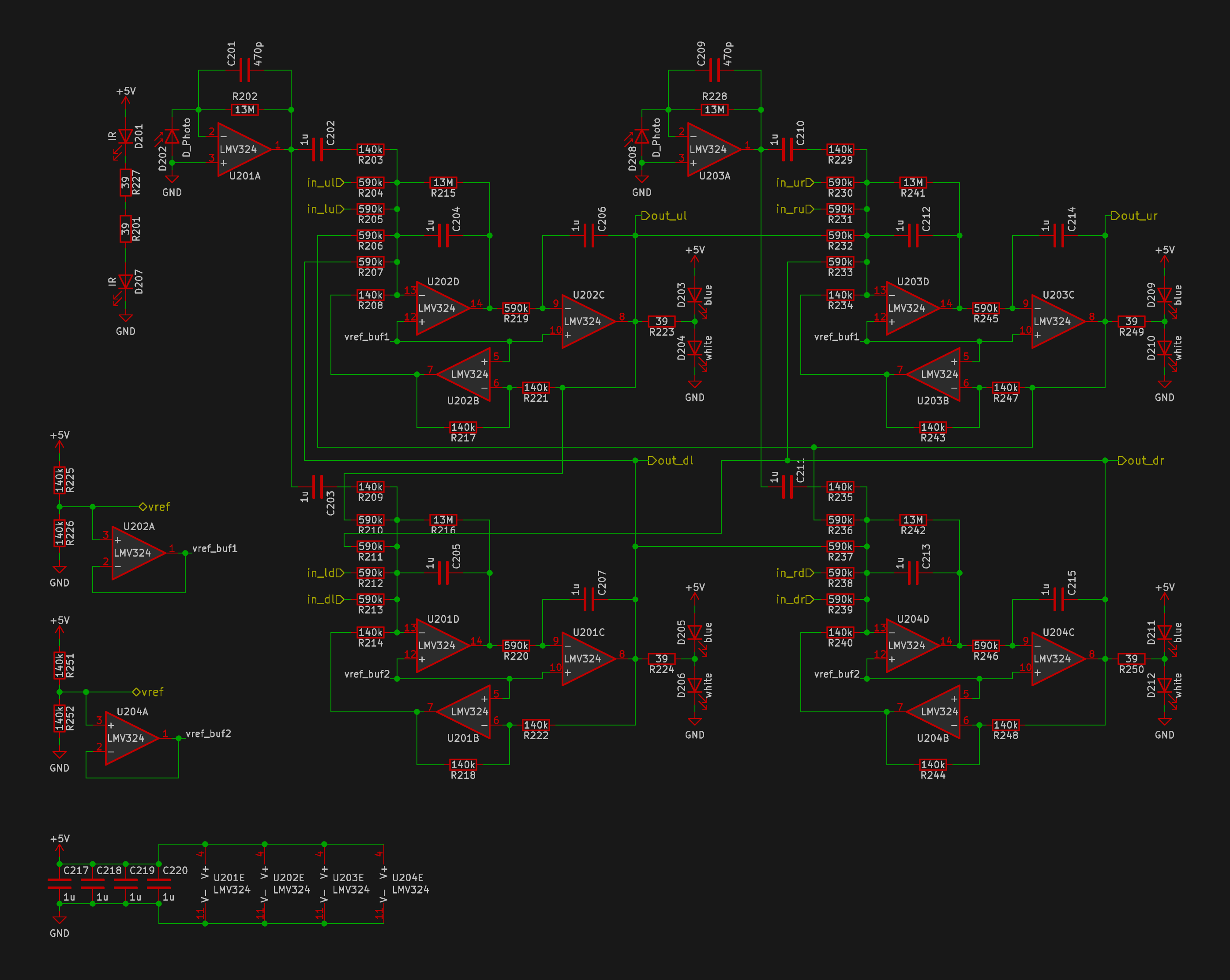 schematic (the good stuff)
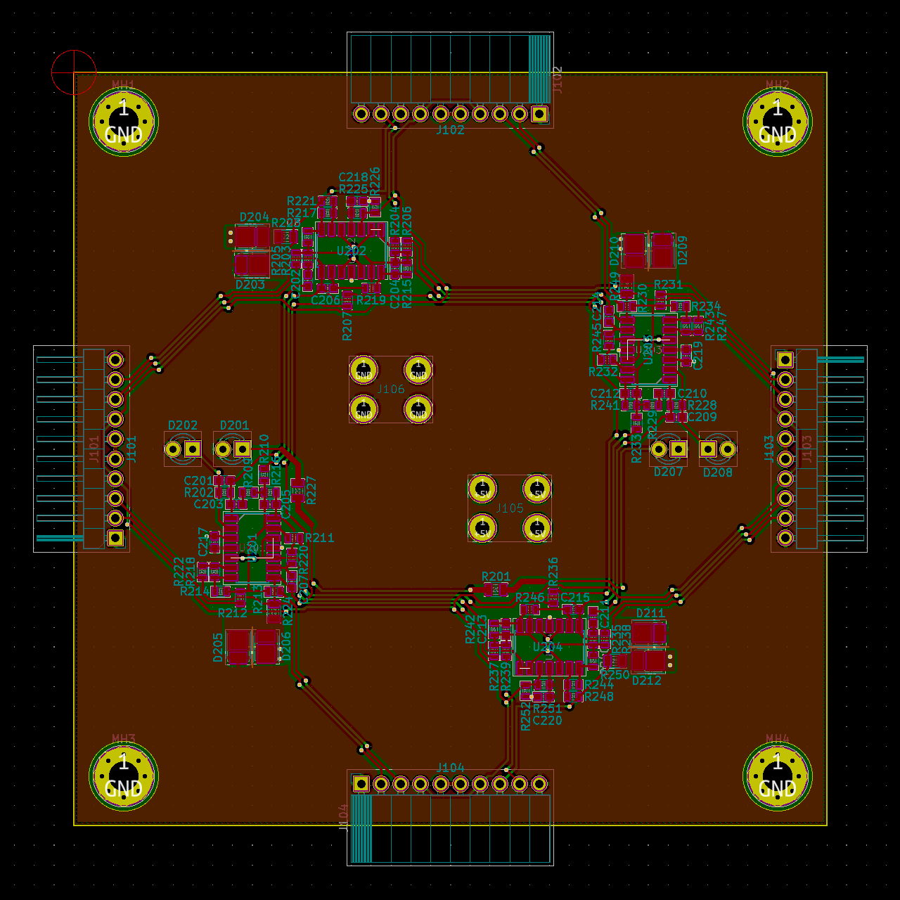 layout
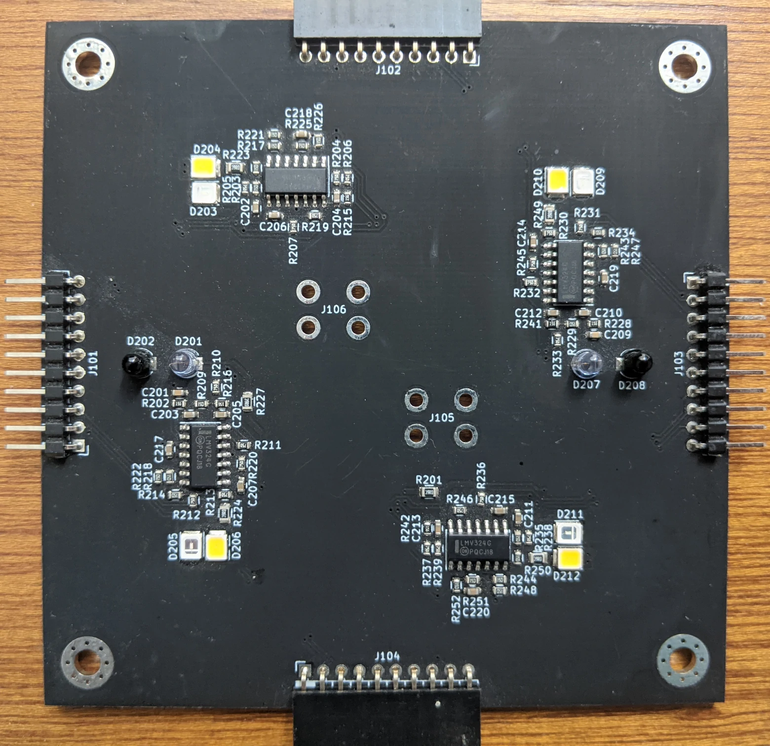 assembled board
The third iteration was a 2D array with four units per board as before, but with a better layout and some extraneous components eliminated. This one used an almost identical circuit to the final version, except one-quarter the size and without a voltage regulator. I made it as a final test for the design and to familiarize myself with the manufacturing process before sending out the real boards.
I upgraded to LMV324DR2G opamps from Onsemi, which have a higher output current and overall better parameters than the previous LMV324LIDT from ST. This allowed me to upgrade to brighter (and oddly, cheaper) LEDs. I also used 0603 passives instead of 0805 for a more compact layout.
I had the boards manufactured by PCBWay, who asked me how each LED was supposed to be oriented. I told them, they made the boards as I specified and shipped them to me, and I discovered that I told them the wrong thing. Oops. I had to reverse every IR LED and photodiode, and killed one in the process, so one of the sensors is non-functional.
This prototype taught me that 1) professionally made boards are really nice and 2) matte black soldermask (at least, PCBWay's stuff) is not very black. I went with glossy black in the final design.