digital PLL SSTC
This project is ongoing.
Following the problems with antenna feedback on SSTC 2, Joshua and I discussed some alternative feedback methods. Sensing secondary base current is another popular way to do it, but it provides a signal that is shifted from the primary voltage by 90 degrees. We could not find any standalone PLLs that can produce a configurable phase shift without lots of supporting circuitry. Combined with the evident need for noise tolerance, we decided that implementing one in digital logic on a FPGA was the way to go.
I have also since moved, leaving SSTC 2 behind. Clearly there is but one choice: build another coil. This one will have the same goals and largely the same design as its predecessor, but it will test a new noise-resistant digital PLL and the use of (much cheaper) IGBTs instead of MOSFETs as primary switches in the driver.
digital PLL
We realized that we needed a PLL with more noise rejection and the ability to control the phase as well as delay of its output. Rather than trying using a PLL chip like the 4046, the PLL for this SSTC uses a field-programmable gate array. As the FPGA is digital, it must produce an output switched on multiples of its internal clock; the design used here runs at 100 MHz, providing more than enough resolution to match a typical SSTC resonant frequency of 100-200 kHz.
controlled oscillator and phase comparator
The oscillator of the PLL emulates a typical VCO, in which a 'voltage' value is added to an overflowing counter every clock cycle. The top bit of the counter is taken as the VCO output. Increasing the value causes the counter to overflow sooner, increasing the frequency of the output. A phase shift is easily added by adding fractions of the counter's maximum value as a fixed offset; if the output counter has 1/4 of its maximum value added to it relative to the internal counter, the output changes state 1/4 cycle (90 degrees) sooner. This relationship does not change with the frequency of the VCO, unlike a fixed delay.
To lock the VCO to the input signal, there is a phase comparator much like phase comparator 2 in the 4046. When a rising edge is seen on the VCO or signal in, the 'voltage' is decreased or increased respectively, until an edge on its counterpart arrives. To compensate for delays in the rest of the circuit, a variable negative delay is introduced by delaying the VCO out to feed into the phase comparator. This is implemented as a simple counter-based delay.
badness rejection
The 4046 has another problem - when the feedback signal is removed, the VCO output drops to the low end of its frequency range. We want the oscillator output to remain at its previous locked state when the signal is shut off. As stated before, we also want the oscillator to ignore noise. To accomplish this, the digital PLL detects when the signal is 'bad' (off or contains spurious edges) and disables the phase comparator for a while until the signal returns. The phase comparator must then use a heavily delayed version of the signal and feedback, to allow the 'bad' signal to cut it off before any noise can reach the phase comparator.
The long delay comes at a cost: the PLL feedback loop becomes unstable and is no longer able to lock to a fixed oscillator. This is not a problem in SSTC usage, because the secondary is only permitted to oscillate at the frequency it is driven at. The feedforward allows the only feedback to be in the form of a phase shift, not a frequency shift, which this PLL can still lock to.
Here's a video of the PLL in action, showing the noise rejection and frequency holding while feedback is shut off. The yellow trace is the PLL out, the blue is the feedback in. Pushing a button on the FPGA board shuts off the feedback, and simulated noise is injected as a burst of pulses every so often.
The annotations may not display correctly here; view on YouTube for best results.
The PLL is far from release ready, but I've put the source code on GitHub for the curious.
IGBT H-bridge
The H-bridge is very similar to the one on SSTC 2 and uses the same board, except the MOSFETs have been replaced by cheaper and hopefully more rugged FGH40N60SMD IGBTs from Fairchild Semiconductor. The IGBTs do not naturally pass reverse current (no parasitic body diode) and have dedicated reverse diodes built in, so the reverse blocking and bypass diodes are no longer needed.
Although IGBTs are frequently used in dual-resonant SSTCs, they have not been used in classic continuous-wave SSTCs as far as I know. The difference may lie in the fact that a DRSSTC has a resonant primary circuit, allowing the switches to only switch when there is no current through them. In classic SSTCs, the primary is not resonant and the switches shut off when the primary current is at its peak. While modern IGBTs are fast and capable switches, their construction makes them less able to handle this type of switching than MOSFETs. From the datasheet it appears that the switch parameters are close enough to those of the FCA36N60NF MOSFETs previously used, but only actual operation will tell if they work or not.
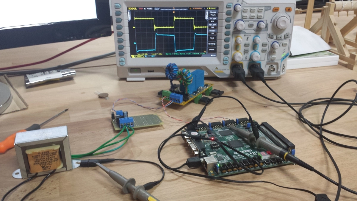 |
A simple test setup, featuring the logic power supply, the FPGA board, the driver board, and a trusty Rigol DS2072. The IGBTs are mounted in small terminal blocks for easy replacement. |
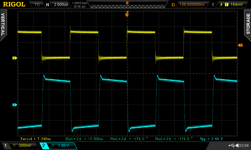 |
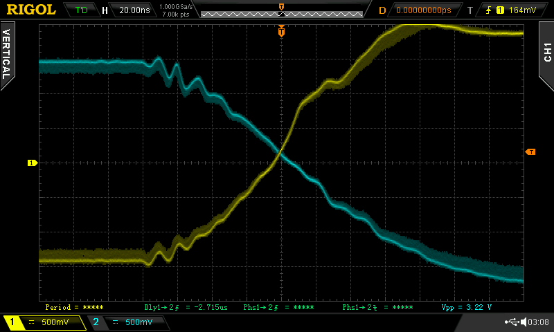
Scope shot of the signal (yellow) and an IGBT gate (blue). The signal is unshielded and appears to pick up noise from the gate drivers as they switch. |
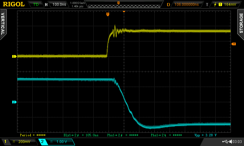 |
Closeup of the previous shot. You can see the noise starting on both the gate and the signal as the gate starts to slew. These gate drivers can switch very hard. |
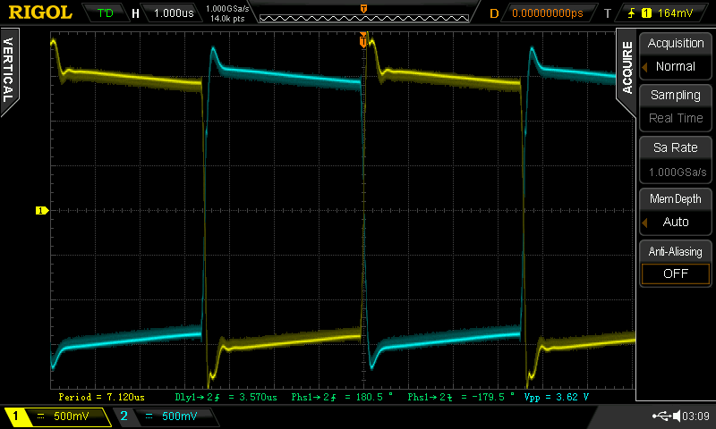 |
Capture of two opposing gates. There appears to be some strange ringing on the yellow trace; I'm not sure what that comes from. |
 |
Closeup of the previous shot. I hope the blips do not affect performance much, and that the fake deadtime is enough for the somewhat asymmetric on/off delays of the IGBTs. |